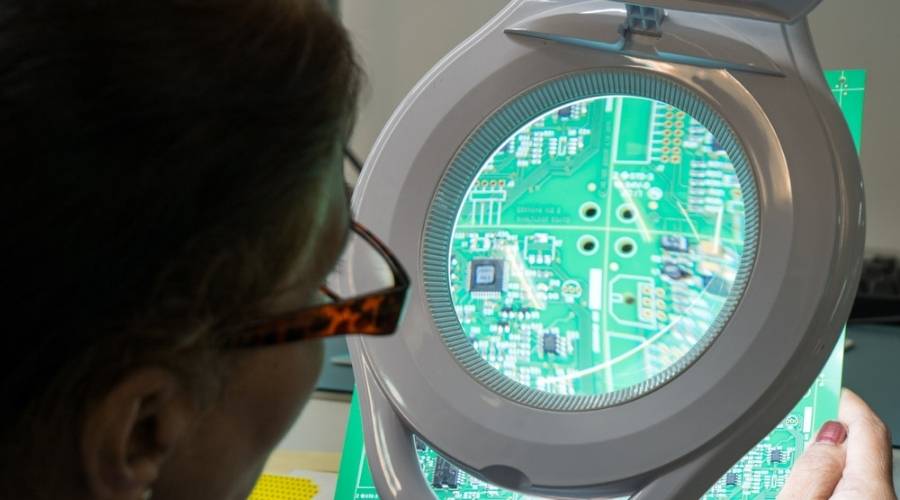
PCB assembly – commonly written as PCBA – is the process of populating a bare printed circuit board with electronic components and soldering them in place to create a functional assembly. It is the central manufacturing process in almost every electronic product, from a simple sensor board to a complex medical instrument or defence system. Understanding what PCBA involves, and what to look for in a contract electronics manufacturer, helps engineering and procurement teams make better decisions about their supply chain.
At NOTE UK, PCBA is one of our core manufacturing capabilities. We deliver it across six UK sites, to ISO 9001 and IPC-A-610 standards, for customers in MedTech, Defence, Industrial, Communications, and GreenTech. This page explains what PCBA is, how our process works, and what makes NOTE UK a reliable long-term manufacturing partner for your assemblies.
What is PCB Assembly (PCBA)?
A printed circuit board (PCB) on its own is just a substrate – a laminated board of glass-reinforced epoxy (typically FR4) etched with conductive copper tracks and pads. It has no function until components are placed and soldered onto it. That process – placing components and creating reliable electrical joints between them and the board – is printed circuit board assembly, or PCBA.
PCBA should not be confused with PCB fabrication (the manufacture of the bare board itself). Fabrication produces the board; assembly populates it. Most contract electronics manufacturers, including NOTE UK, source bare boards from specialist PCB fabricators and then perform the assembly process. Some offer both under one roof; NOTE UK sources bare boards through our supply chain network and focuses on delivering high-quality assembly, test, and integration.
The PCBA Process – Step by Step
Modern PCBA combines automated machinery with skilled human inspection and intervention. The specific steps depend on the technology type – surface mount (SMT), through-hole, or a combination – but the core sequence for an SMT assembly is as follows.
- 1. Solder Paste Application
A stainless steel or nickel stencil, laser-cut to match the PCB pad layout, is aligned over the bare board. Solder paste – a mixture of flux and tiny solder alloy particles – is squeegeed across the stencil, depositing precise amounts of paste onto each pad. Paste volume and consistency are critical: too little and joints will be weak or open; too much and bridges can form between pads. Automated solder paste inspection (SPI) is used at this stage to verify deposit accuracy before any component is placed.
- 2. Component Placement
Pick-and-place machines – high-speed automated systems with multiple heads and vision systems – lift components from reels, trays, or tubes and place them onto the paste-covered pads at high speed and precise coordinates. Modern machines can place tens of thousands of components per hour, achieving placement accuracy measured in hundredths of a millimetre. For fine-pitch devices, BGAs, and other complex packages, vision alignment systems verify placement position before the component is released.
- 3. Reflow Soldering
The populated board travels through a reflow oven – a conveyor system with a controlled temperature profile. The board passes through preheat, soak, reflow, and cooling zones. In the reflow zone, the solder paste melts, the flux activates and cleans the joint surfaces, and the solder alloy flows to create a reliable metallurgical bond between component terminations and PCB pads. The cooling zone solidifies the joints. The temperature profile is precisely engineered to the solder alloy (lead-free or leaded) and the thermal mass of the assembly.
- 4. Through-Hole and Selective Soldering
Not all components are surface mount. Through-hole components – connectors, large capacitors, transformers, and some legacy parts – have leads that pass through drilled holes in the PCB and are soldered on the underside. On mixed-technology boards (containing both SMT and through-hole), the SMT components are reflowed first, then through-hole components are inserted and soldered using one of two methods: wave soldering (the board passes over a standing wave of molten solder) or selective soldering (a programmable nozzle applies solder precisely to individual joints, protecting surrounding SMT components from heat). Selective soldering is the more controllable and increasingly preferred approach for complex mixed boards.
- 5. Inspection
After soldering, every assembly is inspected. The primary method is automated optical inspection (AOI): cameras capture high-resolution images of the board from multiple angles, and software compares the images against the expected component positions, orientations, and joint profiles. AOI identifies missing components, wrong polarity, solder bridges, insufficient solder, and other defects quickly and consistently across the full board.
For assemblies containing BGA (ball grid array) packages, QFN components, or other parts whose joints are hidden under the component body, X-ray inspection is used. X-ray imaging reveals the solder joint formation beneath the package, confirming ball contact, identifying voids, and detecting bridges that optical inspection cannot reach. - 6. Functional Test
Inspection confirms workmanship; functional test confirms that the assembly actually performs as designed. The test method depends on the product and is defined during DFT (Design for Test) planning: in-circuit test (ICT) uses a bed-of-nails fixture to probe component values and connectivity; functional test applies power and stimulates the circuit, verifying outputs against a test specification. For more complex assemblies, boundary scan (JTAG) or flying probe testing may also be used. NOTE UK works with customers to develop and validate test strategies during the NPI phase, so test is designed in – not bolted on after the fact.
PCBA Technology Types
The three main assembly technologies each suit different component types and product requirements.
| Technology | What it means | Typical use |
| SMT (Surface Mount) | Components are mounted directly onto the PCB surface and reflowed. The dominant technology for modern designs. | Most commercial, industrial, medical, and defence PCBAs |
| Through-Hole (THT) | Component leads pass through drilled holes and are soldered on the underside. More mechanically robust than SMT for high-stress connections. | Connectors, power components, legacy parts, high-reliability joints |
| Mixed Technology | Combines SMT and through-hole on the same board — SMT reflowed first, through-hole components soldered subsequently. | The majority of real-world complex assemblies |
PCBA Quality Standards — IPC-A-610 Explained
The internationally recognised workmanship standard for PCB assembly is IPC-A-610, published by IPC (the Association Connecting Electronics Industries). It defines three classes of acceptability, each specifying increasingly strict criteria for solder joint geometry, component placement, and cosmetic acceptability.
| Class | Application | What it means in practice |
| Class 1 | General electronics | Basic functionality is the criterion. Cosmetic imperfections acceptable if joints are electrically sound. |
| Class 2 | Dedicated service electronics | Stricter joint geometry and inspection criteria. Used for most commercial, industrial, and communications products. Extended performance life expected. |
| Class 3 | High-reliability electronics | The most demanding standard. Used for defence, aerospace, and life-critical medical applications where failure is not an option. Zero tolerance for certain defect types. |
NOTE UK applies IPC-A-610 Class 2 as standard across all commercial and industrial PCBA programmes. IPC Class 3 is applied for medical device assemblies under ISO 13485, defence electronics under AS9100, and any programme where the customer specifies it. Our operators and inspectors are trained and certified to IPC-A-610 requirements.
Lead-Free and RoHS-Compliant PCBA
The RoHS Directive (Restriction of Hazardous Substances) restricts the use of lead and five other hazardous materials in electrical and electronic equipment placed on the EU and UK markets. NOTE UK manufactures to RoHS and REACH requirements as standard, using lead-free solder alloys (typically SAC305 – tin, silver, copper) across our production lines.
Lead-free reflow requires higher peak temperatures than traditional tin-lead processes, which has implications for component selection, PCB laminate grade, and oven profiling. Our process engineers manage this during DFM review to ensure component ratings and PCB materials are compatible with lead-free assembly.
Where programmes require leaded (SnPb) assembly – for example, some defence or space applications where RoHS exemptions apply, or legacy products where component availability constrains the BOM – we can accommodate leaded processes within our qualified process capability. This should be confirmed at the quotation stage.
PCBA at NOTE UK – What We Deliver
NOTE UK delivers PCBA across six manufacturing sites in England: Windsor, Haddenham, Basildon, Wolverhampton, and through our STI sites at Hook and Poynton. Our capability covers the full technology spectrum and the full volume range.
Assembly Technology
- Surface mount technology (SMT) – high-speed automated placement and reflow
- Through-hole assembly – manual and automated insertion, wave and selective soldering
- Mixed-technology boards – SMT and through-hole combined in a single programme
- Fine-pitch, BGA, QFN, and other advanced package types
Inspection and Test
- Automated optical inspection (AOI) – standard on all assemblies post-reflow
- X-ray inspection – available for BGA and hidden-joint verification
- In-circuit test (ICT), functional test, flying probe and boundary scan (JTAG) – to customer test specification
- First article inspection (FAI) with documented approval records
Quality and Certification
- ISO 9001 – quality management across all sites
- ISO 13485 – medical device manufacturing
- AS9100 – aerospace and defence (STI, Hook and Poynton)
- IPC-A-610 Class 2 standard; Class 3 available for high-reliability programmes
- Lead-free (RoHS/REACH) as standard; leaded processes available where specified
Volume and Scalability
- Low-volume NPI and engineering prototypes
- Bridge production and ramp builds
- High-volume serial production – scalable across our six-site UK network
- Multi-site capacity for dual-sourcing or volume overflow
Integration with Wider Manufacturing
PCBA at NOTE UK does not exist in isolation. Our manufacturing capability extends to cable and harness assembly, box build and system integration, functional test, and 3PL fulfilment – all managed under one contract. For customers who need a complete product, not just a board, we can take the PCBA output and continue through to a finished, tested, packaged product ready for despatch to your customer.
Sectors We Serve
NOTE UK’s PCBA capability supports customers across five market sectors, each with distinct quality, traceability, and regulatory requirements.
- MedTech – ISO 13485-certified PCBA for diagnostic equipment, patient monitoring, surgical instruments, and life-support systems. Full component traceability, validated processes, and first article inspection as standard.
- Security & Defence – AS9100-certified, IPC Class 3 PCBA for mission-critical electronics. Secure production environments, EMI and environmental test capability, zero-failure-tolerance workmanship.
- Industrial – Durable, long-lifecycle assemblies for automation, process control, and power electronics. Typically IPC Class 2 with functional test to customer specification.
- Communications – High-throughput PCBA for infrastructure, networking, and connectivity products. Scalable capacity and supply chain agility for volume programmes.
- GreenTech – PCBA for renewable energy, EV charging, and energy management systems, where reliability in demanding environments is essential.
How to Work with NOTE UK on PCBA
The fastest way to get an accurate quotation is to provide us with your Gerber files or a full BOM with approved manufacturer parts, assembly drawings, target annual volumes, and any specific quality, certification, or test requirements. Our engineering team will review DFM and DFT considerations at the quotation stage, flagging anything that could affect cost, yield, or lead time before production starts.
We work with customers at every stage: from first prototype and NPI builds, through bridge production, to volume serial manufacture – with the same team, the same processes, and no re-qualification needed as volumes grow.
| Ready to discuss your PCBA requirements? Contact our team via the enquiry form below or email info.note@note-ems.co.uk. We’ll get back to you promptly. |
Frequently Asked Questions – PCBA
A: PCBA stands for printed circuit board assembly – the process of placing and soldering electronic components onto a bare PCB to create a functional assembly. It is distinct from PCB fabrication, which produces the bare board itself.
A: A PCB (printed circuit board) is the unpopulated substrate – a laminated board with conductive copper tracks and pads but no components. A PCBA is the populated assembly: the PCB with all electronic components placed and soldered onto it. The PCBA is what goes into a finished product.
A: SMT stands for surface mount technology the dominant modern method of PCB assembly. Components are mounted directly onto the surface of the PCB and soldered in place through a reflow oven process, rather than having leads that pass through the board. SMT enables smaller components, higher component density, and faster automated placement compared with older through-hole assembly methods.
A: IPC-A-610 is the internationally recognised workmanship standard for PCB assembly, published by IPC. It defines three acceptability classes: Class 1 (general electronics), Class 2 (dedicated service electronics), and Class 3 (high-reliability electronics for defence, aerospace, and life-critical applications). NOTE UK applies IPC Class 2 as standard and IPC Class 3 for medical, defence, and high-reliability programmes.
A: AOI stands for automated optical inspection – a machine vision system that photographs the assembled PCB from multiple angles and compares the images against the expected component positions, orientations, and solder joint profiles. AOI is the primary post-reflow inspection method and identifies defects such as missing components, wrong polarity, solder bridges, and insufficient solder quickly and consistently across the full board.
A: Both are methods of soldering through-hole components on the underside of a PCB. Wave soldering passes the board over a standing wave of molten solder, which wets all exposed pads simultaneously – efficient for boards with many through-hole components in accessible locations. Selective soldering uses a programmable nozzle to apply solder to individual joints, protecting surrounding SMT components and allowing precise control of heat application. Selective soldering is preferred for complex mixed-technology boards.
A: Yes. Lead-free manufacturing to RoHS and REACH requirements is standard across NOTE UK’s production lines. We use lead-free solder alloys (typically SAC305) for reflow and selective soldering processes. Leaded (SnPb) assembly is available for programmes where RoHS exemptions apply or where specific legacy requirements demand it – this should be confirmed at the quotation stage.
A: Yes. Our placement machines handle fine-pitch SMT packages, BGAs, QFNs, and other advanced component types. BGA assemblies are inspected using X-ray imaging to verify ball contact and detect voids or bridging beneath the package body that optical inspection cannot reach.
A: NOTE UK supports the complete volume range – from single-unit prototypes and low-volume NPI builds through to high-volume serial production across multiple sites. Our six UK facilities provide flexible, scalable capacity so customers can grow their volumes without changing supplier.