Key Takeaways
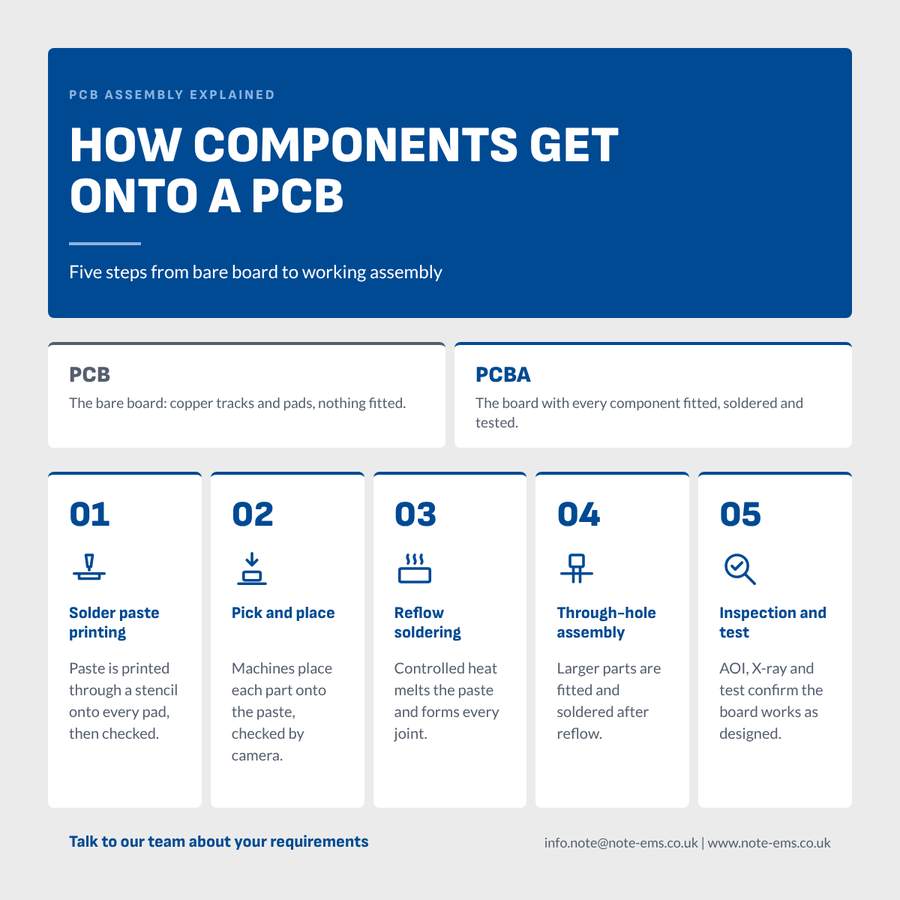
- Components are fitted to a PCB in five steps: solder paste printing, pick and place, reflow soldering, through-hole assembly, and inspection and test.
- A PCB is the bare board. A PCBA is the same board with every component fitted, soldered, inspected and tested.
- Most soldering defects start at the paste printing stage, so paste quality is controlled before any part is placed.
- Inspection and test run through the whole build, not just at the end of the line.
- PCB assembly at NOTE in the UK is built to IPC-A-610, and we match each project to the UK site best suited to it.
Table of contents
- Before the line: data, DfM and sourcing
- Step 1: Solder paste printing
- Step 2: Pick and place
- Step 3: Reflow soldering
- Step 4: Through-hole assembly
- Step 5: Inspection and test
- What to ask your EMS partner
- The same process, from prototype to volume
- Terms used in this post
- Frequently asked questions
- Talk to our team
A printed circuit board (PCB) is the bare board: copper tracks and pads on a laminate, with nothing fitted. A printed circuit board assembly (PCBA) is the same board with every component placed, soldered, inspected and tested, ready to do its job in your product.
The short answer: components are fitted to a PCB in five steps: solder paste printing, pick and place, reflow soldering, through-hole assembly, and inspection and test.
Here is how we do it at NOTE in the UK, and what to ask about each step when you choose a manufacturing partner. For a wider introduction, see PCBA explained.
Before the line: data, DfM and sourcing
Every build starts with your data pack: Gerber files, the bill of materials (BOM), pick and place data and assembly drawings. Our engineers review it with your design team in a design for manufacture (DfM) review. This is where pad sizes, component spacing, test access and hard-to-source parts get picked up, while a change still costs little.
Components are then bought from authorised sources, checked at goods-in and kitted against the BOM. Each batch is traceable from that point through to final test.
Step 1: Solder paste printing
Solder paste is a mix of tiny solder spheres and flux. A laser-cut stainless steel stencil, made to match the pads on your board, is lined up over the PCB, and a squeegee pushes paste through the openings onto each pad.
The amount and position of paste on each pad decides how good the finished joint will be. Too little gives a weak or open joint; too much can bridge two pins. That is why paste deposits are checked before placement, often with automated 3D solder paste inspection (SPI).
Step 2: Pick and place
Pick and place machines take components from reels, trays and tubes and set them onto the wet paste using vacuum nozzles. Cameras check each part’s position and orientation before it goes down, and the paste holds it in place until soldering.
The machines are fast and very precise. Our lines place hundreds of thousands of parts an hour, from chips as small as 01005 (0.4 x 0.2mm, about the size of a grain of sand) up to large processors and connectors.
Step 3: Reflow soldering
The populated board travels through a reflow oven with a series of controlled heat zones: preheat, soak, reflow and cooling. The paste melts, the flux cleans the metal surfaces, and surface tension pulls each component neatly onto its pads.
The temperature profile is set for each board, based on its size, its copper and its most heat-sensitive parts. Double-sided boards go through the print, place and reflow steps once for each side.
For some boards we use vapour phase soldering instead. The board is heated in the vapour of an inert fluid, which gives very even heat and a peak temperature that cannot overshoot. It suits dense boards and boards with large, heat-hungry parts.
Step 4: Through-hole assembly
Some components still have leads that pass through holes in the board: connectors, transformers, large capacitors and parts that take mechanical stress. These are fitted after reflow, which is why most boards today are mixed technology.
Depending on the board, through-hole parts are soldered by wave soldering, selective soldering or by hand by trained operators. Selective and hand soldering protect the surface mount parts already in place.
Step 5: Inspection and test
Inspection is built into the line rather than left to the end:
- Automated optical inspection (AOI) after reflow compares every part and joint with the expected result, picking up missing or misaligned parts, wrong polarity and solder bridges.
- X-ray inspection checks joints hidden under parts such as BGAs and QFNs.
- Visual inspection to IPC-A-610, the industry standard for acceptable assemblies, at Class 2 or Class 3 depending on the product.
- Electrical and functional test, such as boundary scan, flying probe or custom functional test to your specification, confirms the board works as designed.
Where the product needs extra protection from moisture, dust or vibration, boards can be conformal coated before they ship or move on to box build.
What to ask your EMS partner
Every step is a place where quality is won or lost. These are the questions worth asking:
| Step | What can go wrong | What to ask |
|---|---|---|
| Data and DfM | Design issues found late, when changes cost more | Will you review my data pack with my design team before the first build? |
| Solder paste | Too little or too much paste, leading to weak joints or bridges | How do you check paste deposits before placement? |
| Pick and place | Wrong, missing or misaligned parts | What is the smallest and largest part your lines can place? |
| Reflow | Cold joints or heat damage to sensitive parts | Is the reflow profile set for my board? |
| Through-hole | Poor hole fill, or damage to parts already fitted | Which soldering method will you use, and why? |
| Inspection and test | Hidden faults reaching the field | Which inspection and test steps are included, and to which IPC class? |
The same process, from prototype to volume
At NOTE in the UK, prototypes are built on the same lines and to the same standard as production. What you learn at the prototype stage carries straight into volume, and you can grow without changing supplier. Find out more on our Prototyping and PCBA Manufacturing pages.
Terms used in this post
| Term | Meaning |
|---|---|
| PCB | Printed circuit board: the bare board with copper tracks and pads |
| PCBA | Printed circuit board assembly: the board with components fitted and soldered |
| SMT | Surface mount technology: parts soldered onto pads on the surface of the board |
| THT | Through-hole technology: parts with leads that pass through holes in the board |
| BOM | Bill of materials: the list of every part on the board |
| DfM | Design for manufacture: a review of the design so it can be built reliably |
| SPI | Solder paste inspection: a 3D check of paste deposits before placement |
| AOI | Automated optical inspection: a camera check of parts and joints after soldering |
| BGA | Ball grid array: a package with its joints hidden underneath, checked by X-ray |
| IPC-A-610 | The industry standard for the acceptability of electronic assemblies |
Frequently asked questions
What is the difference between a PCB and a PCBA?
A PCB is the bare board with copper tracks and pads but no components. A PCBA is the finished assembly, with every component placed, soldered, inspected and tested.
What is the difference between SMT and through-hole assembly?
Surface mount technology (SMT) parts sit on pads on the surface of the board and are soldered in a reflow oven. Through-hole parts have leads that pass through holes in the board and are soldered by wave, selective or hand soldering. Many boards use both.
Where do most soldering defects start?
At solder paste printing. The amount and position of paste on each pad decides the quality of the joint, which is why paste deposits are checked before any component is placed.
How are hidden solder joints inspected?
Joints under parts such as BGAs and QFNs cannot be seen by a camera, so they are checked with X-ray inspection.
Which NOTE site in the UK will build my board?
Each of our UK sites has its own strengths. Tell us about your product and your requirements, and we will match your project to the site best placed to build it.
Talk to our team
Planning a new board, or looking to move an existing one? Contact our team to discuss your requirements, and we will match your project to the NOTE site in the UK best suited to it. Talk to our team.